
Product Name
Monolayer graphene film, 1 cm x 1 cm on SiO2/Si substrate, avg. no. of layers, 1
Quality Level
양식
film
특징
avg. no. of layers 1
저항성
600 Ω/sq
길이 × 너비 × 두께
1 cm × 1 cm × (theoretical) 0.345 nm, monolayer graphene film
1 cm × 1 cm × 525 μm, SiO2/Si substrate
유사한 제품을 찾으십니까? 방문 제품 비교 안내
관련 카테고리
일반 설명
Graphene film
Growth Method: CVD synthesis
Transfer Method: Clean transfer method
Quality Control: Optical Microscopy & Raman checked
Size: 1 cm x 1 cm
Appearance (Color): Transparent
Transparency: >97%
Appearance (Form): Film
Coverage: >95%
Number of graphene layers: 1
Thickness (theoretical): 0.345 nm
FET Electron Mobility on Al2O3: 2; 000 cm2/V·s
FET Electron Mobility on SiO2/Si (expected): 4; 000 cm2/V·s
Sheet Resistance: 600 Ohms/sq.
Grain size: Up to 10 μm
Substrate
Size: 1.25 cm x 1.25 cm
Type/Dopant: P/B
Orientation: 100
Growth Method: CZ
Resistivity: 1-30 ohmcm
Thickness: 525 +/- 25μm
Front Surface: polished
Back Surface: etched
Coating: 300 nm thermal oxide on both wafer sides
Graphene is a unique one atom thick, two dimensional allotrope of carbon. Among all the synthesis technique, chemical vapor deposition of graphene on various substrates is the most promising route for the large scale production of good quality graphene. Graphene deposited on dielectric surface may exhibit better performance in graphene based FETs. Graphene deposited on SiO2/Si may be deposited by direct chemical vapor deposition via a sacrificial copper film.
Sheet resistance measurements were performed in a vacuum chamber to ensure their reproducibility, within a four-point configuration (van der Pauw geometry, silver paint contact) with injection of currents above 10uA
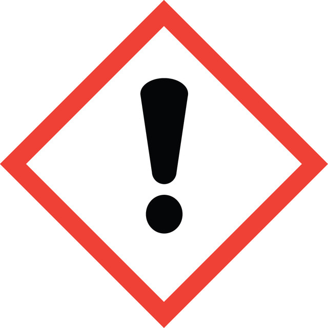
신호어
Danger
유해 및 위험 성명서
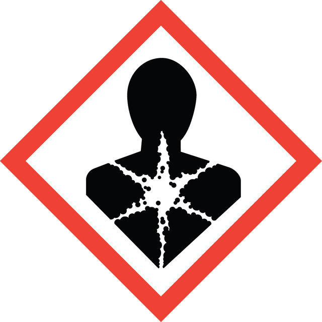
Hazard Classifications
Eye Irrit. 2 - STOT RE 1 Inhalation - STOT SE 3
표적 기관
Lungs, Respiratory system
Storage Class Code
6.1D - Non-combustible acute toxic Cat.3 / toxic hazardous materials or hazardous materials causing chronic effects
WGK
WGK 3
Flash Point (°F)
Not applicable
Flash Point (°C)
Not applicable
자사의 과학자팀은 생명 과학, 재료 과학, 화학 합성, 크로마토그래피, 분석 및 기타 많은 영역을 포함한 모든 과학 분야에 경험이 있습니다..
고객지원팀으로 연락바랍니다.